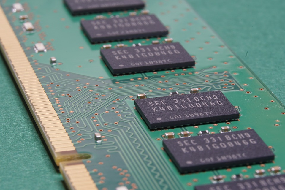
A printed circuit board (PCB) is a circuit board made up of numerous components placed on a solid surface. The printed circuit board has been standardized in design so that one circuit board will fit all sorts of electronic equipment. This allows for small changes to be made on the fly when changing equipment without rebuilding or replacing the equipment. Because of the significant benefit it provides, many small and medium-sized companies choose to outsource their electronic equipment’s PCB inspection and testing to a specialized company. In addition, it makes perfect business sense because the equipment is less likely to break down during transit. The long and short of it is that this saves both time and money.
A printed circuit board (PCB) is basically like a map to a home, allowing the designer to know exactly where every piece of the circuit board goes and what they do. They are also an important component of the assembly process and a critical element of the final testing stage. Several different parties do the PCB inspection process. Firstly, some engineers perform tests on the PCB. They look at the physical properties of the circuit board, how it functions. Additionally, they verify if the schematics which are usually provided with the PCB are correct.
These tests and inspections are vital, but what happens when the equipment breaks down during transit? Some companies use an automated testing method called thermal cycling. The testing method used in this situation is to continuously expose the PCB to high-temperature temperatures and simulate failures along the way.
Another type of inspection that is used is called power semiconductor discharge testing, or SEMD. This testing method involves passing a strong electric current through the PCB, which heats the conductors, creating a short. If the SEMD is conducted continuously for a certain period without changing the physical state of the PCB, the equipment will fail.
Many other methods are used for testing; however, the most important benefit of using a PCB inspection technician is to ensure that the products produced by the manufacturers are defect-free. Since most PCBs are produced with several layers, it is difficult to determine whether one layer is defective without performing a thorough testing process. This method is sometimes referred to as “bio-stacking.” Although this method does not guarantee defect-free products, it significantly reduces the amount of time spent producing a defect-free product. PCB inspection is also useful when determining if a component, such as a bridge is functioning correctly.