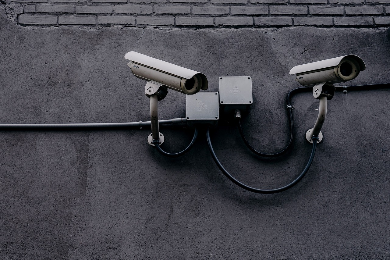
How to Design PCB Layouts for Medical Devices

Designing PCB layouts for medical devices is crucial for functionality and safety. A well-designed layout can enhance performance while providing good protection against interference. Medical device PCB layout design is not an easy task, so some guidelines can help designers achieve success in their projects.

Firstly, designers must follow the industry standards and comply with regulations. Medical devices undergo rigorous testing, so it is important to ensure they meet safety and performance criteria. Thus, designers need to follow the guidelines prescribed by organizations such as The International Electrotechnical Commission IEC and The Food and Drug Administration FDA. These organizations regularly update their safety requirements to ensure high levels of safety and performance.

Secondly, designers should consider components’ placement on the circuit board. When designing a medical device PCB layout, the location of components such as capacitors, resistors, and power inputs should be carefully considered. Signal path lengths and signal integrity are crucial for measurement accuracy, so placing the components’ carefully is important. Signal interference can cause serious mistakes in measurements and possibly hazardous outcomes.

Thirdly, designers should keep the patient in mind when designing a medical device PCB layout. A device’s components should be designed in such a way that they do not cause harm, are reliable, and resistant to errors. Thus, the layout should prioritize a patient’s safety, focusing on both the device’s physical and electrical safety. A well-designed layout can help prevent patients from getting shocked or burned.

Fourthly, designers should choose components that maximize the device’s performance while minimizing interference. While selecting components, designers should consider factors such as cost, temperature rating, and dissipation. A device’s performance can be greatly enhanced by selecting the right components and placing them in the right location with enough space around them. Doing this will ensure good current conduction, reduce the likelihood of short circuits, and help with heat dissipation.

Lastly, designers should consider the size of the circuit board. Size is an important factor in medical devices because they are often small. It is important to design the PCB layout so that it is as small as possible while still retaining circuit functionality. Keeping the layout precise can help minimize the device’s overall size, which makes it more convenient and improves usability.

Medical device PCB layout design is a critical component to ensure safe and efficient performance. The guidance and industry standards provided by organizations such as IEC and FDA help ensure that PCB layouts are safe, reliable, and perform accurately as intended. With careful considerations regarding component placement, patient safety, and performance, designers can create a layout that reduces interference, maximizes efficiency, and enhances overall device functionality. Bearing in mind that a device’s size is an important factor, creating a small and efficient layout can greatly improve a device’s usability while ensuring it is working appropriately. The PCB layout of medical devices plays a crucial role in ensuring safety, accuracy and performance.

Phidget Load Cell: 3 Main Points

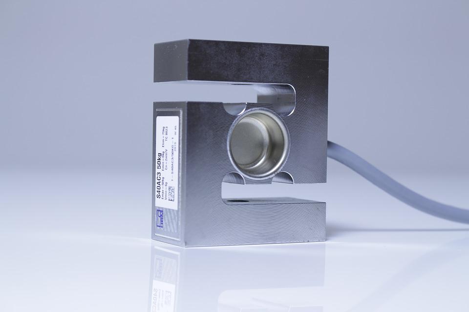
Phidget Load Cell is a device used to measure weight or force. It is usually used in industrial or manufacturing settings but can have other applications as well. In this article, we will discuss three main points about Phidget Load Cell: what it is, how it works, and its applications.

Phidget Load Cell is a device that uses strain gauges to measure weight or force. It is typically used in industrial or manufacturing settings but can have other applications as well. The device works by measuring the amount of deformation that occurs when an object is placed on it. The Phidget Load Cell then converts this measurement into a weight or force reading.

Some common applications for Phidget Load Cell include:

  • Weighingbridge Scales
  • Material Handling Systems
  • Tank and Hopper Weighing Systems
  • Compact Bench Scales

Phidget load cells are accurate, durable, and easy to use, making them a popular choice for many different applications. If you need to weigh or measure force, a Phidget load cell is a great option to consider.

How do they work?

Phidget Load Cells use a technology called piezoelectricity to measure force. When an object is placed on the load cell, it produces a small voltage. This voltage is then amplified and converted into a weight or force reading. Phidget load cells are available in a variety of sizes and capacities, so you can choose the one that best suits your needs.

What are some common applications for Phidget Load Cells?

They are commonly used in weighing bridge scales, material handling systems, tank and hopper weighing systems, and compact bench scales. They are also frequently used in research and development laboratories.

What are they made of?

The Phidget Load Cell is made of aluminum and has a black anodized finish. The Phidget logo is laser-etched into the top surface.

How do I connect it?

The Phidget Load Cell uses four wires to connect to your Phidget controller. Two of these wires are for power (red and black), and two are for the signal (green and white). Make sure to connect the wires according to their corresponding colors. Red goes with red, green goes with green, etc.

What kind of input does it take?

The Phidget Load Cell takes a differential input. This means that it takes two signals: one that is slightly higher than the ground and one that is slightly lower than the ground. When these two signals are combined, the Phidget Load Cell is able to output a very accurate reading.

What is the maximum weight that it can measure?

The Phidget Load Cell has a maximum weight capacity of 50kg. This means that it can accurately measure anything from a few grams to 50 kilograms.

For more information and buying options, check online.

The Layout Of A Custom Circuit Board

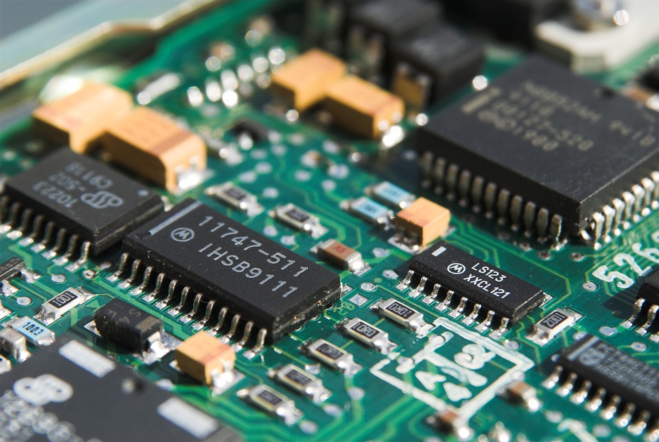
While custom PCB design is possible, it is essential to remember that the layout and construction of the board need to be carefully considered. The final setup must be as precise as possible, yet it must also be compatible with any machining process. Additionally, the board’s structure must be well-engineered to minimize the chance of errors. A qualified team of engineers will be required to design and produce a customized PCB. Depending on the specifications, engineering costs will vary.

The layout of a custom circuit board is an essential element of the design process. The structure must be correct and efficient, so it is essential to understand how the components fit together. It is important to have a detailed schematic since this will help ensure the board works as intended. You can use a computer-aided design program to transfer your schematic into a PCB. Once you have your schematic, you can place your components on the board in the correct location. If the same component is performing the same function in two different places, it is best to have them next.

The layout of a custom PCB can be customized to meet your specific needs. You can even use your design. This is a crucial process that requires knowledge of PCB software and computer-aided systems. Once you have your schematic, you can easily convert it to a PCB and place the components in the proper position. By placing similar elements next, you can quickly identify which parts have identical functions. There is no limit to how you can design a custom PCB to suit your needs.

After determining the size and shape, you can decide the layout. This is an important part of the process. You will have to create a structure in which the parts are organized in a logical order. By defining the schematic, you will be able to build a custom circuit board that meets all of your specifications. In addition, this step will make it easy to manufacture the PCB, as you will be able to see the design as it will look once it is assembled.

Creating a custom circuit board layout is a complex process that requires technical know-how and a computer-aided system. With this, you can transfer your design from a schematic to a PCB, ensuring that it is logical and meets your requirements. You can upload the schematic of your custom circuit board to your manufacturing company. If you are not comfortable with the layout, you can always hire a designer.

Eicr In Watford: Things You Should Know

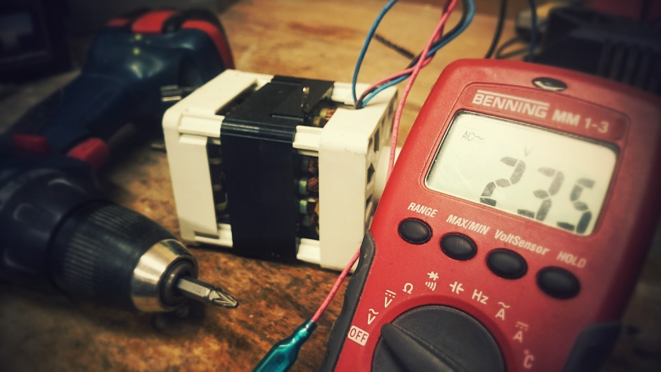
Eicr in Watford is a subject discussed for decades, yet many people don’t know much about Eicr. Eicr stands for Electron-beam Induced Current Recording. Eicrs are used to record the electrical currents caused by ionizing radiation, which can be emitted from sources such as x-rays and radioactive isotopes. We hope this article will help inform you of everything you need to know about Eicr!

1) What is Eicrs

Eicrs are used to record the electrical currents caused by ionizing radiation, which can be emitted from sources such as x-rays and radioactive isotopes. For Eicr Watford, look no further than EICR Partner.

2) What are its benefits?

Eicrs can help people, especially engineers and students, understand more about Eicr. Your results can also be used to pinpoint areas that require improvements in Eicr insulation or security of the Eicr system.
EICR Partner is an expert Eicr company based in London with a team of dedicated technicians who are qualified members of the IET (Institution Of Engineering And Technology). They’re available 24/07 for all your Ecr testing needs!

Eicr has been around for almost 100 years. However, some people still don’t know what it involves or whether they need one done on their Ecr system – which can indicate some problems that may affect the performance or safety of your home. The most common reason for ECR inspection is when you’re buying a property because an Ecr report carries more weight than other types of surveys, making it easier to get mortgages approved too!

3) What are its disadvantages?

Although much less common than x-rays, there are some health risks associated with ionizing radiation because it has sufficient energy to break chemical bonds in molecules – which may lead to cancer after long-term exposure at high doses. This is why EICR Partners should carry out eicr. They are certified professionals with the required knowledge and experience to carry out Eicr testing safely.

4) Important things you should know about Eicr

First, EICR testing can reveal the location of any electrical problems such as damaged cables and faulty connections. This allows EICR to identify potential hazards that could cause severe injury or even death if not detected quickly enough. Second, EICRs play a vital role in determining whether your home insurance policy will cover you should an incident occur at your property – because it’s more likely to be covered by your insurer (and pay up) when no hidden dangers are lurking around the place!

Eicr in Watford test report carries more weight than other surveys, making it easier to get mortgages approved too! It also provides peace of mind knowing exactly what issues need to be resolved before moving into your new home. Eicrwill also identifies if any illegal or unsafe modifications have been made to the building, such as ground floor extensions without planning permission – which could pose a potential health and safety risk.

We hope this information has been helpful to you.

A Brief On Prototype Circuit Board

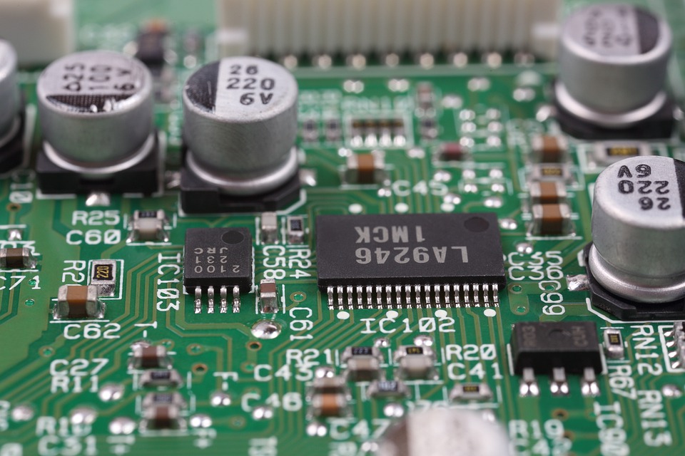
A prototype circuit board is a fully functional printed circuit board. These boards are used to test new designs or as finished products themselves. Prototype PCBs are the first step in any printed circuit design, and they are typically made using printed conductors on sheets of thin insulating material plated through holes.

A schematic diagram describes how the electrical components and connections work. This is then converted into a printed circuit board by creating the circuit pattern and etching it onto a material such as fiberglass-reinforced epoxy or copper laminated onto an insulating substrate.

There are two types of prototyping: one-offs where boards are built for one-time use and small batches (or assemblies) where boards are built in quantity but not enough to qualify for volume pricing.

The conductors on the prototype circuit board are created by making an image of the pattern on the copper foil with a photosensitive material and covering it with a developed resist so that areas of bare copper remain while other areas are etched away. It’s more complicated to make a prototype circuit board than to make a one-off because the alignment of the pattern must be precise. This is difficult when you are routing connections between components that may only be 1/16 inch apart after they are assembled into the finished product.

Once completed, many companies remove chips from their PC boards for testing purposes (and resolder them later) because it’s much easier to troubleshoot the board with all parts in place.

Technological advances now allow companies to take digital pictures of their boards, load them into a software program, and have the boards fabbed by an outside supplier.

There are two major types of prototype circuit boards: single-sided and double-sided. Single-sided boards are constructed by etching the copper foil from one side of the board only. Double-sided boards require that connections be made between opposite sides to connect all layers.

A Prototype Circuit Board offers many benefits. They are often the first step in designing a PCB. Many times, companies need to test their products before they are mass-produced. Using a prototype circuit board allows for this testing to be done without having to wait on large quantities of product that may or may not work as required. Also, these help with the speed and savings of not having to use as many resources. Today more companies are using Prototype Circuit Boards to do their testing because of the many benefits.

Best Mobile Hot Water Heater

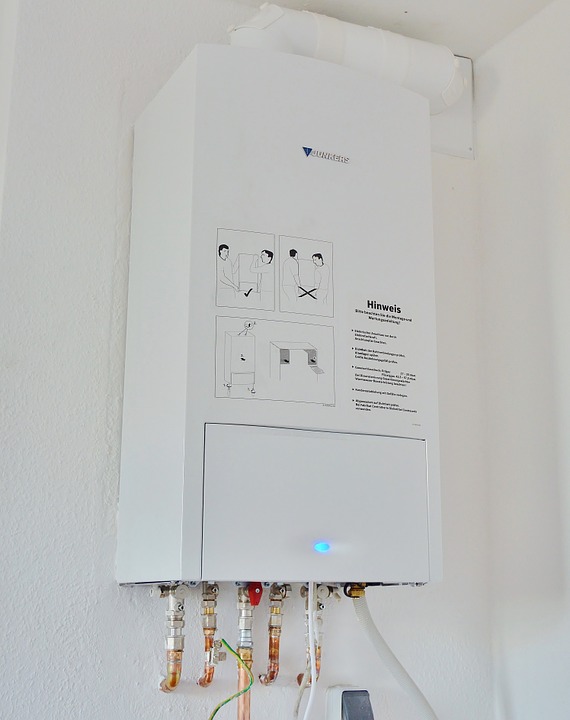
There’s a lot to love about the great outdoors. However, a cold shower just isn’t one of them. It’s not fun to clean up and splash around when you are shivering uncontrollably. You can say goodbye to this unpleasant experience when you start to camp out with a water heater. Mobile options are now available for people who love to hike, fish, and hunt for days. You can keep yourself clean and have an easier time doing basic chores around the camp. If you want to find the best mobile hot water heater, then be sure to check the following:

Portability

The unit may have to be lugged around a considerable distance depending on the campsite’s proximity to the trailhead. Sometimes this is several miles of hiking. You are already bringing lots of other gear so you will probably appreciate a more portable solution. Compare various products in terms of volume and weight. It would also be nice if the product comes with its own carrying bag with pockets for cables and accessories.

Ease of Use

It should not take a genius just to operate this best mobile hot water heater. The controls must be intuitive such that even children can use them without issues. Find one with an LCD display, if possible, so that you can see the current water temperature setting at any given time. It should also be easy to power this on. The electronics will generally require a 12V source which could be from the RV, an outdoor generator, or other power solutions.

Safety Features

Although this heater uses gas, you don’t have to worry much because using it outdoors allows any exhaust fumes to dissipate into the air instead of creating problems for the users. Most of these will also have built-in systems to prevent failure. They can monitor the temperature and turn off the burner if the water reaches a certain temperature. They have fuses in case of power fluctuations and water flow sensors that can prevent further damage. You can read the reviews as well to see comments on safety.

Reliability

You will be far from help when camping so you need each piece of gear and equipment to work without any issues. Check what other people are saying about different products. Were they able to rely on these every time? Did they encounter any difficulties? Does the water temperature get hot enough for their liking? Does it work even at high altitudes? Can the pump deliver enough water pressure?

PCB Inspection For PCB Manufacturers

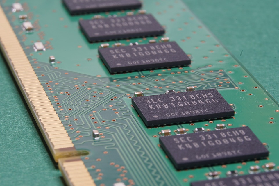
A printed circuit board (PCB) is a circuit board made up of numerous components placed on a solid surface. The printed circuit board has been standardized in design so that one circuit board will fit all sorts of electronic equipment. This allows for small changes to be made on the fly when changing equipment without rebuilding or replacing the equipment. Because of the significant benefit it provides, many small and medium-sized companies choose to outsource their electronic equipment’s PCB inspection and testing to a specialized company. In addition, it makes perfect business sense because the equipment is less likely to break down during transit. The long and short of it is that this saves both time and money.

A printed circuit board (PCB) is basically like a map to a home, allowing the designer to know exactly where every piece of the circuit board goes and what they do. They are also an important component of the assembly process and a critical element of the final testing stage. Several different parties do the PCB inspection process. Firstly, some engineers perform tests on the PCB. They look at the physical properties of the circuit board, how it functions. Additionally, they verify if the schematics which are usually provided with the PCB are correct.

These tests and inspections are vital, but what happens when the equipment breaks down during transit? Some companies use an automated testing method called thermal cycling. The testing method used in this situation is to continuously expose the PCB to high-temperature temperatures and simulate failures along the way.

Another type of inspection that is used is called power semiconductor discharge testing, or SEMD. This testing method involves passing a strong electric current through the PCB, which heats the conductors, creating a short. If the SEMD is conducted continuously for a certain period without changing the physical state of the PCB, the equipment will fail.

Many other methods are used for testing; however, the most important benefit of using a PCB inspection technician is to ensure that the products produced by the manufacturers are defect-free. Since most PCBs are produced with several layers, it is difficult to determine whether one layer is defective without performing a thorough testing process. This method is sometimes referred to as “bio-stacking.” Although this method does not guarantee defect-free products, it significantly reduces the amount of time spent producing a defect-free product. PCB inspection is also useful when determining if a component, such as a bridge is functioning correctly.

Why PCB Inspection Is Necessary

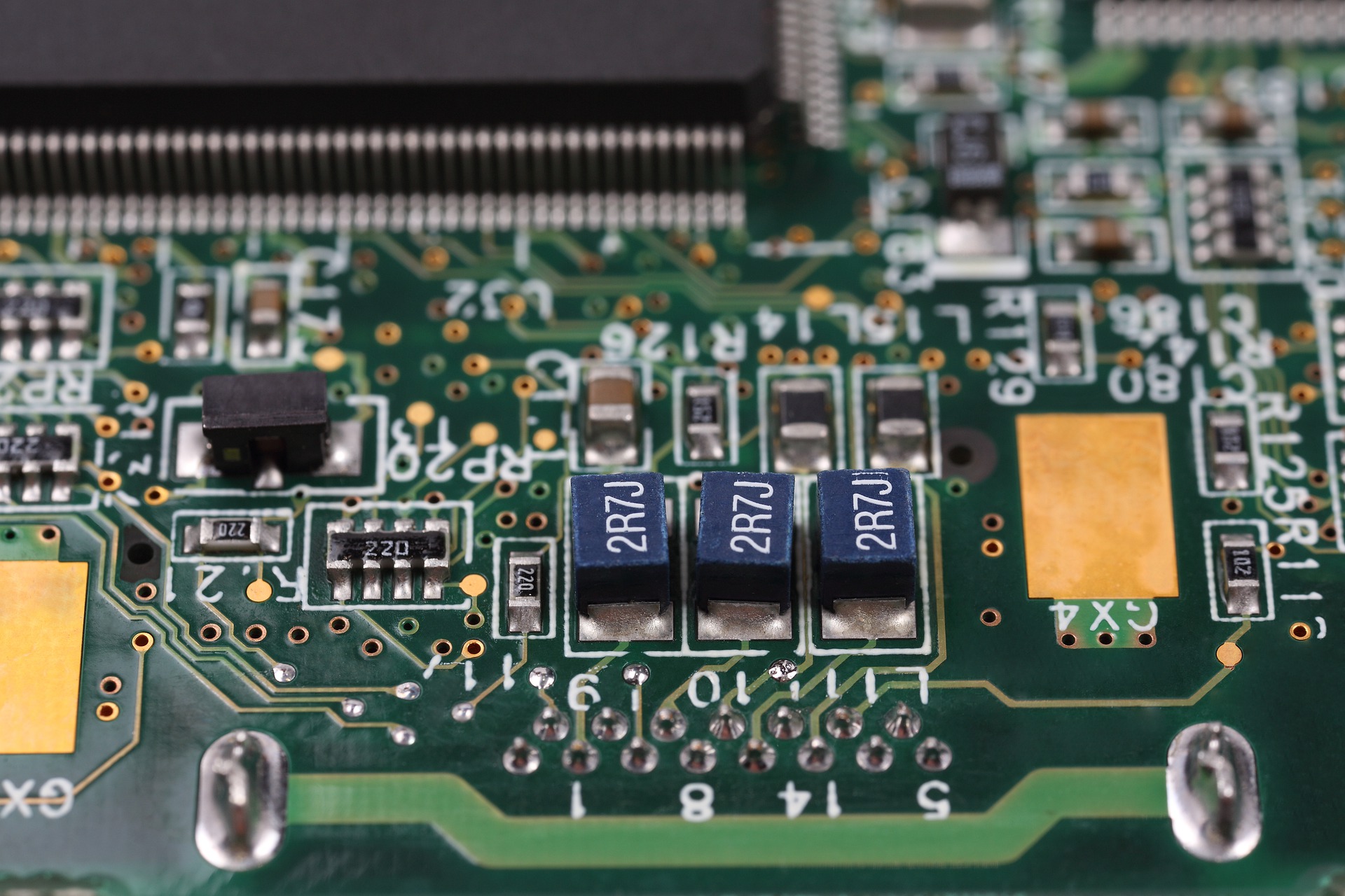
A printed circuit board(PCB) is used for mechanical support and electrical connection in electrical components by means of conductive pathways, signal traces or tracks from copper sheets laminated on a non conductive substrate. It was invented by Paul Eiser (Austria, 1941). PCB works as the foundational device of modern day electronic devices. It can be single layered board as in garage door opener, 6 layered in smart watch and as much as 60 layered in super computers. All the electrical components of a device are integrated by means of this board. Resistors, semi conductors, wheatstone bridge, diodes and capacitors are interconnected to one another and can communicate through PCB. These are widely useful in all of the modern day electronic devices ranging from smaller hearing aids to MRI, CT Scan machinaries, Aerospace monitoring tools, Super computers etc. PCB enables a single operating tool to regulate and manage all the electrical operations in a circuit.

PCB inspection is the necessary element in the manufacture of PCB. It evades all the possibilities of detected errors in default devices later on. To be used in smaller or larger electronic devices, PCB inspection facilitates the error reduction in modern day complex boards.
The various techniques used to undergo PCB inspection are:

-Manual Inspection: It is enabled by minute and detailed Inspection by engineering inspectors to survey any problem or error in the design of board. This method was used earlier in lack of automation devices and was very costly and time consuming. Repeated inspections were to be made that increased the chances of faluts after every inspection.

-Automated Optical PCB Inspection : This smart method involves a series of optical images where the image of a perfect assembly is compared to the image of the model to be inspected. It determines any faults with much accuracy.

-Automated X Ray Inspection: With the evolution of multi-layered boards as in super computers, the optical scanning of PCB has become very difficult. It is almost impossible to observe all the solder joints. The solder joints are must to be observed in new set ups to ensure proper joints. X Ray imaging has overcome this problem to inspect high density PCB. Automated X Ray Inspection detects the tracks, joints and signals from the hidden layers also. This method is little expensive but is the only option to find out defects in manufacture of high density PCB.

PCB inspection facilitates early detection of any manufacturing defects, directing the board for correction of defect before passing on to the next stage. This minimizes the wastage of time and cost required to remove the defect in next more complex stage of production. It enables the proper functioning of an electronic device managing all the assets of electronic components on an error free PCB.

Turnkey PCB Assembly Services – What Are The Benefits Of This Service?

What is Turnkey?

Turnkey refers to a completed product or service which is ready for immediate usage by the buyer. This case implies that the manufacturer will deal with all aspects of the entire PCB design. Essentially, a turnkey solution enables you to control designing PCBs while the provider manages the remainder of the operations. Turnkey PCB assembly Services offer you a complete solution that includes PCB design, prototyping, tooling, and even test runs. This provides a comprehensive way of getting your very own PCB done for a fraction of what it might otherwise cost you to get a brand-new design done. As such, it is one of the most cost-effective ways to get yourself a new PCB that you can use right away.

Benefits of Turnkey Services

There are some benefits that you stand to gain from availing of turnkey PCB assembly services. For starters, it helps you cut back a lot on your initial capital expenditures as well as the time required for getting your web designed and built. The fact that you don’t have to pay any upfront costs also means that you don’t need to spend on labor for this job. If you can set up an online quoting system, you can get an accurate online quote instantly. Some of these quotes will be of lower costs than what you would have had to pay to have someone draw up a custom design for your PCB. You can easily do a little bit of comparison shopping here to make sure you have chosen the best provider for your needs.

Working with a Single Vendor

Another great benefit of full Turnkey PCB assembly Services is that you don’t have to bother yourself with managing multiple vendors for your PCB. The entire task can be entrusted to one single vendor, which would reduce the cost involved with sourcing the materials and the labor for the assembly. So if one person handles the whole assembly, you don’t have to waste time managing the logistics and finances for that person and the delivery of materials.

Find Fully Integration with Software Tools

As far as the software is concerned, you can find several PCB assembly service providers who offer end-to-end products along with their software. You can easily integrate the software with your electronic designing tools and start producing turnkey web designs almost immediately. This is certainly going to help you speed up your production process in a big way. Most of these providers even provide you with PCB layout design templates to easily generate a design based on your requirements.

The most important thing is to get in touch with a good PCB manufacturer who can provide you high quality printed circuit boards at the most competitive prices. But before selecting a manufacturer, you should always keep certain things in your mind like, whether they are offering customized service, their past records.

Reasons To Try Online PCB Manufacturing

A lot of small businesses are dabbling into electronics. Students, enthusiasts, and engineers are also fold of making their own projects. Many of these will require circuits of various complexities. In the past, people were content to making these manually through traditional methods particularly during the prototyping and testing phases. Now it is possible for anyone to get their designs transformed into high quality printed circuit boards thanks to online PCB manufacturing. Below are just a few reasons to try this service:

More Options Leading to Competitive Prices

You may have a few options in your area if you live in large cities. Even so, the prices may be quite high compared to your budget. Consider looking at online options to expand your range. You will find that there are so many more companies that can serve you and give you what you need. Best of all, most of these will charge lower fees than the companies that you are currently engaged with.

Better Logistics Leading to Fast Deliveries

One of the biggest reasons why people didn’t even think about using the services of faraway companies before is that deliveries used to take so long to complete. Back in the day, you would have to be prepared to wait for weeks or months to see the fruits of your labor. That is simply too long to wait. Now this can be cut to a matter of a few days with expedited shipping.

Small to Large Batch online PCB manufacturing Possible, PCB assembly equipment requires a huge investment. Previous methods made the manufacturing of each design an expensive undertaking. It did not make financial sense to accept order for anything but large runs. Now the technology has made it easier to make PCBs in small batches. Many are accepting orders that are as little as one piece. Of course, most would probably want to order more to make it easier to test and trace issues.

Read Service Reviews for Recommendations

If you are worried about the quality of PCBs provided by a company that you have never tried, then look into reviews of their services. There are plenty of satisfied and dissatisfied customers online. Check third-party review sites, engineering forums, and personal blogs that tackle the subject. Perhaps they have mentioned the name of a company that you are interested in. Read what they have to say and learn from their experiences.